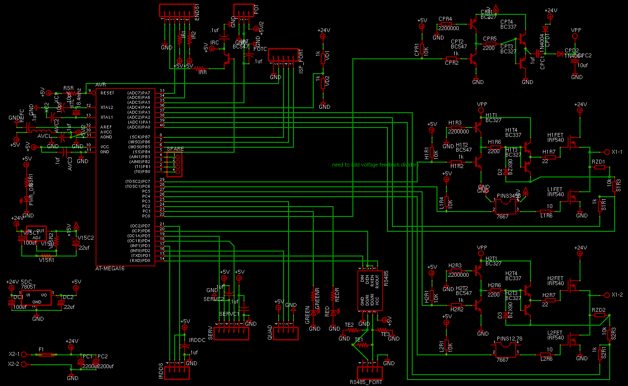
Sensor-less Fet element DC motor driver.
The PCB design was designed in cadsoft eagle using the non-profit license
the circuit card is 125mm*95mm double sided through plated.
The PCB and project code is GPL and the right to use the PCB and code firmware
is free for non-profit users.
Commercial, Educational, government users are asked to contact me if they are interested in using this PCB and code.
Anyone planning to build one is recommended to email me for construction notes on the the latest version board in cvs.
 I often have spare parts and boards or may be able to may also be able arrange a bulk PCB or and parts order if enough people are interested, so please email if interested in this.
Parts List for version 2.xx circuit board.;
Browse CVS web access to robotx files repository PCB file for this
project.;
Browse CVS web access to robotx files repository avr C code files this
project.;
The intention of the board is to provide a
relatively cheap, solution to implementing low or high power servo and
drive systems using conventional DC motors.
After having designed and building a dual motor controller i have found that as simple as it seems controlling a single motor is enough trouble for even a relatively fast 8 bit micro controller, and i don't expect to continue further development of that avenue. The low cost of micro controllers makes it unnecessary to do so. The RS485 bus linked multiple nodes of single controllers each operating it's own feedback loop and motor provide a better solution to controlling complex arms or robotic systems and additional elements can easily be added to extend the system the RS485 standard allows more than enough nodes to be connected to control the most complex of robotic systems.
A wide variety of sensors can be connected and coupled with the processing power
of the AVR micro controller to implement many servo systems
or drive configurations for robotics or other applications. Standalone
use of the system is possible. Though my primary
intention is that it be used as a slave to another system connected by an RS232 to
RS485 bridge circuit.
This board can drive one reversible dc motor, implements regenerative
breaking,and is set up to use sensor less feedback for improved motor control.
As an aside from this it can be used for practically any low voltage (10 to ~50
volts) power switching application.
The circuit board has been tested running from a 24 volts into an RC motor and
tested up to 17amps holding current, and to 14 amps for a resistance load.
Even the low resistance FET's used get nice
and warm at high currents and consistently i suggest that should it be necessary
to run continually at these types of at currents that appropriate heat-sinking be
used. At peak loading of 27amps(IRF540's) the FET power dissipation will be 50
watts each so a considerable sized heat sink should be used. For 24 volt
operation output power of 500 watts for each bridge should be quite easily
handled especially if only for short bursts as could be expected in a robotics
application. I am pretty pleased with the performance so far, i have not yet
managed to break it with a variety motors or resistance loads, the FET's in use are
IRF 540's.
Being a micro controller controlled system it also has the
capability of connecting up to and performing a variety of other simultaneous or
complimentary functions such as handling several quadrature encoders, multiple
switch sensors, can drive RC servos at 12 bit resolution , IRDDS sensors (sharp
GP2D02), analogue potentiometers,and prototyping areas to fit opto coupled
inputs, temperature sensors or GAL or PAL devices, SPI device's such as high
speed ADC or other functionality, the early version board has a number of small
3 and 4 pin connectors setup for various uses while the latest version has a
single 26 pin expansion header and a 14x23 grid prototyping area.
Sensor-less control and PWM drive pattern
The bridge driver software I have written for this hardware
generates PWM at 8.9Khz when running with an 18.4Mhz clock, or 10.7 khz when
running with a 22.1184Mhz clock , is thus able to
drive low inductance motors efficiently.
The drive feedback voltage ADC conversions are auto triggered and
timed to provide voltage and current samples from each bridge in turn. Current
is sampled at the end of the drive pulse when it will have reached it's peak
value, voltage is sampled before the beginning of the pulse to get most accurate
generator voltage at this point. This ADC timing relies on the repetitive nature
of the current pulses to produce a type of oversampling ADC effect (equal to
having a 150khz ADC), this minimizes processing requirements and allows the use
of the AVR's internal 10 bit 15khz ADC speed especially considering the drive
frequency. The current and voltage ADC samples once gathered are processed by a
feedback routine, the driver under development uses this information to control the FET bridges
duty cycles, switches automatically between regenerative breaking and drive and changes directions to control
the motor speed and torque.
Software features.
The Software has been written in a modular fashion , each .c file
encapsulates own functionality, i have setup the Makefile to easily
produce code for several target applications which i am developing including a spot welding timer,
generator bike , differential drive for robotics, miniature monorail carridge controller.
Optional modules for
infra red remote control , and infra red digital distance sensors can be enabled
by defining IDRRS_CODE or/and IIRX_CODE defines.
The Main code provides uart communications routines, eeprom initialization capability with
an eeprom operating system for changing and setting startup parameters for any application in the eeprom,
an adc conversion capability , serial to parallel digital IO routines ,RC servo pulse generation,
stepper motor pulse generation, some diagnostic register and memory display routines.
Pulse Switching Drive frequency is setup for 8.9Khz with an 18.4mhz avr clock.
(could be reduced to as low as 63hz or increased to an estimated upper
limit of around 20khz). The switch frequency chosen is usually based on the
motor inductance. Higher frequency will reduce switching and resistance motor
losses while maximizing torque and speed. If frequency is set too high switching
losses will become a factor. Frequency can be changed to suit various motor
and drive arrangements.
Current limiting and generator voltage based
feedback from the motor can then be used to provide feedback to control the
speed of the motor without using any other sensors at all, this is known as
sensor less control, this can provide an additional degree of control over motor
speed and torque which cannot be achieved with a simple variable PWM drive, or
even by the use of expensive encoders on the motor. So even while quadrature
or pulse width control is also in use this capability can provide additional
current limiting and overload protection, or robustness in cases of sensory failure which enables the motors to be driven
continually at their maximum torc and peak power without damaging them.
To achieve this complex sampling and processing task the ADC code has it's own
interrupt conversion state machine which processes ADC samples in a linked list
to provide the sensorlesscurrent and generator voltage feedback. The ADC samples
are auto-triggered using output compare 1B. The ADC auto triggering allows precise timing needed to perform the
conversions, and the flexibility of the linked list allows insertion other adc
conversion requests while running the bridge routines.
The bridge element switching state machine also runs a linked list system which
contains the 4 FET element switch states and timing information to provide for practically any
switching pattern to be implemented as well as the ability to smoothly change
patterns from for example forward acceleration to forward regenerative
breaking thanks to the triple buffer system providing an intervening
wait-transitional state. The bridge driver code uses one 8 bit timer, and in
each timer cycle will process all the switching steps necessary to control the
4 FET bridge elements. The linked list is pre generated and sorted to provide
switching patterns to drive the motor by a separate routine.The H-bridge
linked list generation ,system handles the changeover and state changes between
stop, reverse, and forward and forward or reverse regenerative braking, it is
fully comprehensive in it's ability to control a motor. And the transitional
states ensure clean changeovers from one state to the next.
.
Construction Notes and Circuit operation
The Mega16 or
Mega32 avr processor is programmed in system, the simplest way is using the uisp
utility program with a parallel port cable with 4 wires directly to the
ISP_port on the circuit board.
The AVR's UART hardware adapts to an RS485 (ds75176) driver IC, I usually run the
communications at 115200 baud. RS485 interface allows multiple devices
on a single buss (software permitting) thus allowing multiple controller
boards to operate on one buss possibly as slave nodes to a single PC serial port.
The uart communications receive and transmit
operations run under their own interrupt's, and circular buffers hold the data.
Port C7,C6,C5,C4 drive the H bridge elements, The FET element control algorithm in the
software generates fail safe switching sequences to account for FET gate
charge-discharge times otherwise the fuse, circuit board ,power fets or other
components may be damaged.
ADC Ports are used for feedback from the bridge outputs 2 lines from each side this is intended to allow measuring both high level or low level voltages at the feedback points.
These allow bridge fet-current measurement based on the voltage drop across the ON
state resistance of the low side FETS used (this needs to be calculated based on
the type of FET used), and also allow the higher generator voltage
to be measured to determine open circuit speed of the motors,and regeneration
voltage measurement.
The high side fet voltage pump (see IC VU and surrounding components)
uses discreet transistors to produce a 15 volt square wave output ,
which adds an additional 10 to 15 volts to the main supply and so can provide
the high side FET gates with the on state voltage required. The higher frequency
of the pump the greater the current it can provide.
The bridge output elements are N channel fets, the driver stages will drive most
power FETS suggested devices are IRF540 (100volt, 27 amp .04ohms) or stp55ne06
(60volt ,55amp.022ohms). The board tracks are only large enough to provide a current capability of around 10 amps and thus it is intended that should a higher
current IE 15 amps be required the circuit tracks should be reinforced by addition of copper braid or wire to increase the copper CSA.
The fets are laid out inline so that a single heat sink can be
used if needed otherwise the copper plated board will provide sufficient heat-sinking to handle currents up to around 10 amps.
The High side bridge driver circuitry is explained as follows.
The transistor T2 (H1T2) is used as a constant current source and is setup for a
nominal current of ~3.6 miliamps for a 24 volt system. In the off state
the T2's collector is pulled low by T1 (H1T1) to about .2 volts in this
state T2 dissipates 140mw of power. The output of the T1-T2 arrangement can thus
switch between .2 and 39 volts with a nearly unlimited sink current through T1
and a 3.6 milliamp source current from T2.
The T3-T4 arrangement is a push pull
emitter follower , it is driven via R3 (2.2K ohm resistor) from the T1-T2 stage.
It can sink or source large currents to charge and discharge the high side
fet gates. The 2.2k resistor R3 limits the current drawn by the T3-T4 stage in
the off state to a worst case of 12 milliamps (.25watts dissipated by R3). The
zenner diode prevents the gate voltage rizing to high to quickly when switching
on and prevents the base voltage of T3-T4 exceeding specifications
when being switched off.
The lowest current dissipation is obtained by turning all the high side
elements off when the bridges
are not is use. This limits the bridges current/power dissipation to around 8
milliamps which is the current drawn by the 2 current source transistors.
The current could be reduced somewhat by
changing values of some of the resistors, the present values are optimized for
at work performance rather than reducing standby current.
The transistors and Circuit components shown are limited to a maximum supply
voltage of ~34 volts dc.as the bs327 and bs337 are only 45 volt rated,and bs556
bs546 are only 65 volt rated,thus limiting the maximum supply to ~34 volts.
By substituting higher spec components such as 2n5550 and 2n5401 transistors
and different resistors in the high side driver circuitry it should be possible
to operate it to as high as 80 volts. If adapted for a 48-50 volt setup even with the same IRF540 fets this could drive Resistance loads of over 1000 watts.
The low side FETS are driven by a DS0026 or ICL7667 dual driver ic.
This High side fet drive driver circuitry has good frequency response is
relatively simple but is effective for the intended application, High side
driver IC's are becoming readily available now but transistors still work very well and are
easily available and cheap.
The 5 volt supply arrangement uses a lm7805T regulator
The 15 volt supply is done with an LM317T
Various feedback systems are setup with a range of ports and connectors on the far edge of the circuit card, including switch , quadrature and potentiometers inputs and even IRDDS connectors.
Ports D2, D3, B2 and B3 are useful for quadrature encoder or pulse inputs
as they all have individual AVR interrupt vectors.
 ;
;
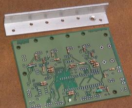
Heat sink assembly i use a 20x20 x3mm aluminum angle drilled to match the board.
 ;
;
Picture of partially assembled board ready for intermediate testing.
 ;
;
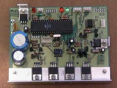
Picture of a completed assembled and tested avr drive board.


